Posts

Showing posts with the label 3

Simple 3 Volts FM Transmitter Schematic

Image
This is a simple and useful circuit diagram of an FM transmitter is sown in this schematic . This FM Transmitter software is very simple and it has a acceptable transmission . The signal transited from this FM transmitter can be received at almost 300 meters in open air The circuit require a 3volts operating voltage and can be tuned anywhere in the FM band. 3V FM Transmitter Circuit Diagram You can use this emitter circuit to transmit signal from your house to garden or from room to room . To listen the signal you can use any radio (portable or not ) that can work on FM band . Connect a half or quarter wavelength antenna (length of wire) to the aerial point. At an FM frequency of 100 MHz these lengths are 150 cm and 75 cm respectively. The calibration of this FM emitter circuit is very simple and you need just to place a radio at some distance from the transmitter and set it somewhere about 88-107MHZ( chose the transmission frequency ) and after that vary the transmitter oscillator fre...

3 phase induction motor

Image

LTC3601 3 3V DC Power Converter Circuit Diagram

Image
This Dc power converter circuit is designed LTC3601 from Linear Technology and is capable to up to 1.5A output current at a 3.3V. The LTC3601 operating supply voltage range is from 4V to 15V making it suitable for a wide range of power supply applications. The operating frequency of the LTC3601 buck regulator is programmable from 800kHz to 4MHz with an external resistor enabling the use of small surface mount inductors. LTC3601 3.3V DC Power Converter Circuit Diagram The LTC3601 buck regulator can operate in two modes: Burst Mode operation and forced continuous mode to allow the user to optimize output voltage ripple, noise, and light load efficiency for a given application.

Mushkin Atom 3 0 USB flash drive introduced

Image
I am quite sure that by now, many of us have already amassed quite a collection of USB flash drives over the months and years that have gone by. Hardly any conference or road show is devoid of a USB flash drive which more often than not contains the press release of a particular company, or a portfolio of new products. Having said that, it can be pretty difficult trying to keep track of just where exactly have you placed that particular file over in the myriad of USB flash drives that you have in your collection, and instead get a personal USB flash drive for yourself so that you can keep personal things private and secure. Just in case you are in the market scouting for a new USB flash drive, have you considered checking out the Mushkin Atom 3.0? The Mushkin Atom 3.0 USB flash drive will place plenty of emphasis on convenience, where it comes in an extremely small form factor which is slightly less than the size of your average quarter. All of this without having to sacrifice on perfo...

30 VDC Stabilized power supply with current control 0 002 3 A

Image
  General Description This is a high quality power supply with a continuously variable stabilised output adjustable at any value between 0 and 30VDC. The circuit also incorporates an electronic output current limiter that effectively controls the output current from a few milliamperes (2 mA) to the maximum output of three amperes that the circuit can deliver. This feature makes this power supply indispensable in the experimenters laboratory as it is possible to limit the current to the typical maximum that a circuit under test may require, and power it up then, without any fear that it may be damaged if something goes wrong. There is also a visual indication that the current limiter is in operation so that you can see at a glance that your circuit is exceeding or not its preset limits.     Technical Specifications - Characteristics Input Voltage: ................ 24 VAC Input Current: ................ 3 A (max) Output Voltage: ............. 0-30 V adjustable Outp...

3 Input Video MUX Cable Circuit Diagram

Image
The circuit diagram shows a low-cost 3-input video MUX cable driver. In this circuit, the amplifier is loaded by the sum of RF and RG of each disabled amplifier. Resistor values have been chosen to keep the total back termination at 75 Ω while maintaining a gain of 1 at the 75-Ω load. The switching time between any two channels is approximately 32 ns when both enable pins are driven. When designing a circuit board for this cable driver, care should be taken to minimize trace lengths at the inverting input. The ground plane should also be pulled away from RF and RG on both sides of the board to minimize stray capacitance. Current consumption of the cable driver is a modest 8mA. 3-Input Video MUX Cable Circuit Diagram 

Simple 3 volt to 9 volt with LMC555 Circuit Diagram

Image
Simple 3 volt to 9 volt with LMC555 Circuit Diagram . This is a Build a 3 volt to 9 volt with LMC555 Circuit Diagram. This dc converter is built with the CMOS version of 555 timer. You can get 12V too if you change the zener diode to a 12V version. 3 volt to 9 volt with LMC555 Circuit Diagram

Build a Voltage to Frequency Converter Circuit Diagram 3

Image
Build a Voltage to Frequency Converter Circuit Diagram 3 . The input voltage, V1, causes C1 to charge and produce a ramp voltage at the output of the 741 op amp. Diodes D1 and D2 are four-layer devices. When the voltage across C1 reaches the breakover voltage of either diode, the diode conducts to discharge C1 rapidly and the op amp output goes abruptly to zero. This rapid discharge action applies a narrow pulse to G1 and G2. Positive discharge pulses produced by a positive V1 are coupled to the output only through G1, while negative pulses are coupled only through G2.  Because of the forward break-over current of diodes D1 and D2, the circuit won`t operate below a minimum input voltage. An increase of R1 increases this minimum voltage and reduces the circuit`s dynamic range. The minimum input voltage with R1 at 1 Kn is in the range of 10 to 50 m V. This input dead zone, when input signal V1 is near zero is desirable in applications that require a signal to exceed a certain level b...

Mini Amplifier with 3 Transistor

Image
Mini 3 transistor amplifier is a simple amplifier with 50mW power drawn by 3 transitor. The series of three mini-amplifier transistors can be used for loud speaker 8 ohm load. Source voltage required to activate the mini-amplifier can be drawn from the batteries 9V.Rangkaian 3 transistor amplifier is often used in simple portabe audio devices such as radios or small tape recorder. Mini-transistor amplifier circuit 3 is quite simple as shown in the figure below. Mini-transistor amplifier circuit 3 includes type of amplifier OTL (Output Transformer Less). Mini-transistor amplifier circuit 3 is used for output coupling capacitors. Amplifier circuit is simple and suitable when used for audio amplifier experiment.

Hofner Colorama II restoration project part 3 re fretting the guitar neck

Image
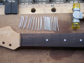
In the last blog post, we stripped down and de-fretted a vintage Hofner Colorama II neck. Today we’ll re-fret it. First of all, we need to do some initial preparation, so we lay the neck out on its jig just like in the previous post and then sort out the fret wire. These frets have been bought pre-cut and pre-radiused. They’re not all the same length, so we need to sort them in order of shortest to longest. Here we’ve punched holes (don’t use the frets to do this!) in an empty cardboard box and placed the frets in them in the correct order. Next thing we need to do is clean all of the dust, etc., out of the fret slots. A thin craft knife will suffice for this, but do it in the opposite direction to the knife edge (in other words, if the blade is pointing forwards, then pull the knife backwards). Remember, we’re not actually cutting anything here, just pushing all of the dust out of the slots. Next we take our shortest fret and do a test fitting in the first fret slot. Uh-oh, it seems t...

Using LTC3601 3 3V DC Power Converter

Image
This Dc power converter circuit is designed LTC3601 from Linear Technology and is capable to up to 1.5A output current at a 3.3V. The LTC3601 operating supply voltage range is from 4V to 15V making it suitable for a wide range of power supply applications. The operating frequency of the LTC3601 buck regulator is programmable from 800kHz to 4MHz with an external resistor enabling the use of small surface mount inductors. Using LTC3601 3.3V DC Power Converter  Circuit Diagram The LTC3601 buck regulator can operate in two modes: Burst Mode operation and forced continuous mode to allow the user to optimize output voltage ripple, noise, and light load efficiency for a given application.

Using LTC3601 3 3V DC Power Converter

Image
This Dc power converter circuit is designed LTC3601 from Linear Technology and is capable to up to 1.5A output current at a 3.3V. The LTC3601 operating supply voltage range is from 4V to 15V making it suitable for a wide range of power supply applications. The operating frequency of the LTC3601 buck regulator is programmable from 800kHz to 4MHz with an external resistor enabling the use of small surface mount inductors. Using LTC3601 3.3V DC Power Converter Circuit Diagram The LTC3601 buck regulator can operate in two modes: Burst Mode operation and forced continuous mode to allow the user to optimize output voltage ripple, noise, and light load efficiency for a given application.

Universal Tester for 3 pin Devices

Image
Most 3-terminal active components can be  tested statically using just an ohmmeter. But  when you have a lot of these devices to test,  the procedure soon becomes boring. That’s  where the idea came from to combine fast,  easy testing for these types of device into a  single instrument.  The unit described here enables you to test  NPN and PNP bipolar transistors, N-or Pchannel FETs or MOSFETs, UJTs, triacs, and thyristors. Regardless of the type of device, the  tests are non-destructive. Universal connectors allow testing of all package types, including SMDs (up to a point). The unit lets you  change from one type of device to another in  a trice. It avoids using a multi-pole switch, as  they’re too expensive and hard to find.  . Circuit diagram : Universal Tester for 3-pin Devices Circuit Diagram . Here’s how to build a versatile instrument at  a ridiculously low cost. IC1 is a 4066 quad CMOS switch which will let u...

3 Watt power amplifier schematic

Image
This time I will share a circuit of schematis power amplifier with LM380 IC that has similarities with LM384. Enough with just a few components you have to make this power amplifier circuit . All components with relatively low prices and making a fairly easy. For this amplifier output power has 3W with 4 ohm impedance. Indeed , this amplifier has the output is quite low and certainly will not be maximal if it works on the speakers with high power. Component List : Resistor R1______________47K R2______________2.7R 2W Capacitor C1______________10uF C2______________470uF C3______________100n C4______________100n IC IC1_____________LM380 , LM384

Build a 3 Channels Audio Splitter Amplifier Circuit Diagram using TL084

Image
This is the schematic diagram of 3 channels audio splitter amplifier circuit which built using op-amp IC TL084. The 3 channels amplifier output distribution applies a single TL084.   3 Channels Audio Splitter Amplifier Circuit Diagram The very first step is to capacitive coupling having a p. 1.0 ~ electrolytic capacitor. The entries are railways Vee Y2 or 4.5 V. This enables working with an individual 9V power source. A voltage gain of 10 (1 M?/100 Kohm) is obtained in the first stage, as well as the other three floors are connected as a unity gain voltage followers. Every single output stage drives independently through an amplifier output 50 pF capacitor towards the resistance of 5.1 k ohm load. The response range is flat from 10 Hz to 30 kHz.

3 Reasons for welding

Image
Reasons for welding of contactor Contact welding occurs only during closing of contacts or during opening and immediate reclosing of contacts because of following reason 1) Inrush currents exceeding making capacity 2) Unstable control voltage 3) Use of diodes as surge suppressors 4) Transition times too low 5) End of electrical endurance Note: These reasons are explain in well detail in concern heading

2 3 Watt Low audio power amplifier

Image
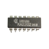
These amplifiers using IC KA2202 and KA2207, which has a power output of 2.3 Watt berimpedansi 4 ohms. Minimum supply voltage and maximum 5Volt 20Volt. See schematics and component list below. Part List  R1 = 100K R2 = 56R R3 = 56R R4 = 1R Use 1/4 Watt resistor C1 = 100uF C2 = 100uF C4 = 100uF C5 = 470uF C6 = 100nF C7 = 470pF C8 = 2,2nF C9 = 100uF U1 = KA2202 , KA2207

PIC16F887 877 programming in C Tutorial 3 1 Timer 0

Image
Timers Both PIC16f887 and 877 have three timers; timer 0, timer 1, and timer 2. Timer 0 is 8-bit and can also be use as counter, Timer 1 is 16-bit timer as well as a counter, where as Timer 2 is 8-bit timer and can be used as the PWM time base for the PWM mode of the CCP module(s).  Timer 0: The Timer0 module timer/counter has the following features: 8-bit timer/counter Readable and writable 8-bit software programmable prescaler Internal or external clock select Interrupt on overflow from FFh to 00h Edge select (rising or falling) for external clock Timer mode is selected by clearing bit T0CS (OPTION_REG<5>). In Timer mode, the Timer0 module will increment every instruction cycle (without prescaler). Counter mode is selected by setting bit T0CS (OPTION_REG<5>). In Counter mode, Timer0 will increment either on every rising or falling edge of pin RA4/T0CKI. The incrementing edge is determined by the Timer0 Source Edge Select bit, T0SE (OPTION_REG<4>). Clearing bit T...

Nmos Power Amplifier Series Part 3

Image
 Nmos400 A power amplifier module capable of up to 400 watts into a 4 ohm load depending on power supply and the output mosfets used.  The layout makes use of older style TO3 mosfets. Nmos400-TO3 Schematic Nmos400-TO3 Layout Nmos350 Mk2 This revised version yet to be built improves a few perfomance areas. I considered more complex ideas but this increased the component count and original idea of the amp would have been lost; that is a powerful high quality amplifier that used commonly available and cheap components. A LED as the voltage reference for the first stage constant current source tracks changes in temperature slightly better that than the old double diode setup. A cascode second stage makes it faster and more linear. Better clipping attributes The fuse has been shifted out of the voltage drive loop between the driver and output stages. Nmos350 Mk2 Schematic

3 Level Audio Power Indicator Circuits Diagram

Image
This circuit is designed to indicate the power level output of any audio amplifier. It's simple, portable, and displays three power levels can be adjusted to any desired value.   3 Level Audio Power Indicator Circuits Diagram Parts: R1__________100K    1/4W Resistor R2___________50K    1/2W Trimmer Cermet R3__________330K    1/4W Resistor R4____________ 1M2   1 /4W Resistor R5__________470K    1/4W Resistor R6 ,R7 _______500K    1/2W Trimmers Cermet R8____________ 1K5   1 /4W Resistor R9-R11______470R    1/4W Resistors   C1___________ 47pF   63V Ceramic Capacitor C2__________ 100nF   63V Polyester Capacitor C3___________47µ F   25V Electrolytic Capacitor C4____________1µ F   25V Electrolytic Capacitor   D1______BZX79C5V1 5.1V 500mW Zener Diode D2_________1N4148   75V 150mA Diode D3-D5________3mm.   Yellow LEDs   IC1_________ LM339   Quad Voltage Comparator IC...