Posts

Showing posts from May, 2017

TOUCH SWITCH CIRCUIT USING NE555

Image

Automatic 9 volt Battery Charger Circuit Diagram

Image
Good care given to your NiCad batteries will ensure a long life. However, they do need to be handled and charged with special care. It is therefore important to first discharge the NiCad to 1 Volt per cell, ensure that the battery is discharged, and then start the charge cycle. recommend a charge current of 1/10th the capacity for a duration of about 15 hours uninterrupted. In reality, we learn some hard lessons when we forget to switch the charger off after the 15 hours and find that one or more cells inside the battery no longer accept a charge. That is the very reason that the circuit above is fully automated. The only thing to do is connect the battery and press the 'Start' button. When the discharge cycle is finished the circuit switches over to charge for 15 hours. After the 15 hours the circuits maintains a trickle charge to keep the battery 'topped-up Automatic 9-volt Battery Charger Circuit Diagram Before I go into the schematic details I like to explain some of th

A Doorbell for the Deaf

Image
This circuit provides a delayed visual indication when a door bell switch is pressed. In addition, a DPDT switch can be moved from within the house which will light a lamp in the door bell switch. The lamp can illuminate the words "Please Wait" for anyone with walking difficulties.  A Doorbell for the Deaf Circuit Diagram : Notes : The circuit uses standard 2 wire doorbell cable or loudspeaker wire. In parallel with the doorbell switch, S1, is a 1N4001 diode and a 12 volt 60mA bulb. The bulb is optional, it may be useful for anyone who is slow to answer the door, all you need to do is flick a switch inside the house, and the bulb will illuminate a label saying Please Wait inside the doorbell switch or close to it. The double pole double throw switch sends the doorbell supply to the lamp, the 22 ohm resistor is there to reduce current flow, should the doorbell switch, S1 be pressed while the lamp is on. The resistor needs to be rated 10 watts, the 0.5 Amp fuse protects agains

Simple FM stereo decoder circuit using MC1310P IC

Image
Simple FM stereo decoder circuit using MC1310P IC via next.gr

Mobile Car Stereo Player

Image
Using a mobile phone while driving is dangerous. It is also against the law. However, you can use your mobile phone as a powerful music player with the help of a stereo power amplifier. This does away with the need of a sophisticated in-dash car music system. Most mobile phones have a music player that offers a number of features including preset/manual sound equalisers. They have standard 3.5mm stereo sockets that allow music to be played through standard stereo headphones/sound amplifiers. Nokia 2700 classic is an example. Circuit diagram : Mobile Car Stereo Player Circuit Diagram A car audio amplifier with 3.5mm socket can be designed and simply connected to the mobile phone output via a shielded cable with suitable connectors/jacks (readymade 3.5mm male-to-male connector cable is a good alternative). Fig. 1 shows the circuit of car stereo player. It is built around popular single-chip audio power amplifier TDA1554Q (IC1). The TDA1554Q is an integrated class-B power amplifier i

Persistence of Vision POV Coding using PIC16

Image
In this section i will tell you about the POV coding using PIC16F877A in C language. Persistence of vision is the phenomenon of the eye by which an afterimage is thought to persist for approximately one twenty-fifth of a second on the retina. My plan is to use the fan from PC power supply; for rotating purpose. Now first of all i want to tell the two things. 1st i don't have smaller MCU that is why me using 40 pin, you can also use 28 pin if you have any. 2nd due to my hardware design fault, actually soldering fault,  i missed the RB0 pin; so to compensate it i used RD0. You can change the coding if you want for your ease. Now come towards the hardware part; as already told you using the 877A MCU with 4MHz crystal, and 16 small leds, 9v dc battery, and one fan. Also don't forget to install the on/off switch to save the battery power. Software part consist of coding in HITECH compiler and there is about 2ms delay after each display. Tricky part in POV coding is to display; for t

Filters 2 way Cross over to your sound system Circuit Diagram

Image
Audio crossovers are a class of electronic filter used in audio applications. The circuit above is a schematic of 2-way Cross-over to your sound system, the crossover is a device used to filter and divide the audio frequency between the bass, midrange and treble. It helps in sound quality, eliminating the distortion that occurs when there is a passage of undue frequencies for a particular speaker. Filters 2-way Cross-over to your sound system Circuit Diagram  

Fading Red Eyes Circuit

Image
Description:  This circuit is used to slowly illuminate and fade a pair of red LEDs (light emitting diodes). The fading LEDs could be installed as 'eyes' in a small pumpkin or skull as a Halloween attraction, or mounted in a Christmas tree ornament. Or, they might be used as a fancy power indicator for your computer, microwave oven, stereo system, TV, or other appliance. In operation, a linear 3 volt (peak to peak) ramping waveform is generated at pin 1 of the LM1458 IC and buffered with an emitter follower transistor stage. The 22uF capacitor and 47K resistor connected to pin 2 establish the frequency which is about 0.5 Hz. You can make the rate adjustable by using a 100K potentiometer in place of the 47K resistor at pin 2. The circuit consists of two operational amplifiers (opamps), one producing a slow rising and falling voltage from about 3 volts to 6 volts, and the other (on the right) is used as a voltage comparator, the output of which supplies a alternating voltage swit

Samsung Galaxy S5 confirmed for MWC

Image
  While rumours have started to swirl over whether or not Samsung will reveal their much-anticipated Galaxy S5 smartphone at Mobile World Congress later this month, the organizing committee has confirmed that they will indeed. Samsung recently sent out invitations to Samsung Unpacked 5, to be held at Mobile World Congress, and an accompanying video hinted that visitors might get a glimpse of the device. While it wasn’t confirmed, Mobile World Live confirmed the rumours. “Samsung is set to launch its Galaxy S5 smartphone at Mobile World Congress this month, having announced its Unpacked 5 event will be held in Barcelona. The company will hold an event on the evening of Monday 24 February, marking the first time it has unveiled a flagship device at the event since the Galaxy S2 in 2011,” they said. Late last year several media houses pegged the reveal around March with a consumer launch in April, but Mobile World Live said that the date has been brought forward – for several reasons.

Little Door Guard Circuit Diagram

Image
If some intruder tries to open the door of your house, this circuit sounds an alarm to alert you against the attempted intrusion. The circuit (Fig. 1) uses readily available, low-cost components. For compactness, an alkaline 12V battery is used for powering the unit. Input DC supply is further regulated to a steady DC voltage of 5V by 3-pin regulator IC 7805 (IC2). Fig. 1: Circuit of the door guard Assemble the unit on a general-purpose PCB as shown in Fig. 4 and mount the same on the door as shown in Fig. 3. Now mount a piece of mirror on the door frame such that it is exactly aligned with the unit. Pin configurations of IC UM3561 and transistors 2N5777 and BC547 are shown in Fig. 2.  Fig. 2: Pin configurations of UM3561 and transistors 2N5777 and BC547 Initially, when the door is closed, the infrared (IR) beam transmitted by IR LED1 is reflected (by the mirror) back to phototransistor 2N5777 (T1). The IR beam falling on phototransistor T1 reverse biases npn transistor T2 and IC1 do

Simple 12V Portable and Mobile Power Supply Schematic

Image
This is the Simple 12V Portable and Mobile Power Supply Schematic .This type of power supply can be built quite inexpensively and needs only a minimum of circuitry. This circuit will give output current of 1 amp, well stabilized and smoothed. Simple 12V Portable and Mobile Power Supply Schematic The smoothing and regulation is provided by IC1 7812 which is a 12V monolithic voltage regulator. Thisportable power supplyunit incorporates output current limiting and is therefore not damaged by accidental short term short circuits or other forms of output overloading.   components Resistor1/3 watt 5% R1 1.8k Capacitors Cl 2200uF 25V electrolytic C2 100nF polyester (C280) C3 100nF polyester (C280) Semiconductors ICI uA78I2 (12 volt 1 amp positive regulator) D1 to D4 1N4002(4 off) Switch S1 DPST toggle type Transformer T1 Standard mains primary, 15 — 0 — 15 volt 2 amp secondary

Alkaline Cell Charger Circuit Diagram

Image
This is the Simple Alkaline Cell Charger Circuit Diagram . This charger works as two channel current limited voltage source 1.6 V. Low charge current allows charging deep discharged cells (0.7 - 0.8 V) and non-rechargeable cells. Charge current can be changed by R9 and R10. With 470 Ohm is approx 7 mA. LED1 and LED indicates when cell voltage reached 1.6 V and cell is fully charged.  If power supply is disconnected, reverse discharging current is negligibly (less than 1 microA). For this feature is operational amplifier type LM324 recommended or similar type with p-n-p transistor on input. Non-rechargeable cells can be charged, but their capacity will be significantly less than rechargeable cells Alkaline Cell Charger Circuit Diagram     Parts list R1 2,2 kohm R2 10 kohm R3 2,7 kohm R4 15 kohm R5, R6 5,6 kohm R7, R8 22 kohm (viz text) / depend on R9, R10 (approx. 50 times greater than R9, R10) R9, R10 470 ohm (see text) / change charge current R11, R12 1 kohm (

Microphone Circuit Test Oscillator Diagram

Image
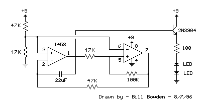
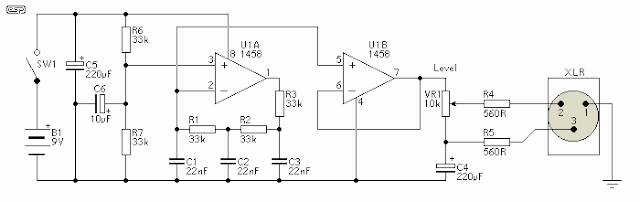
Description This unit would be mounted in a small plastic or preferably metal box, with a 9V battery, level control, a male XLR connector (same as on a mic) and a switch.  Current drain is low, since the circuit only uses one dual opamp.  There is no need for a high quality device, and a 1458 is all that is needed. Circuit Diagram The first stage is the oscillator itself.  This is a simple three stage phase shift oscillator - a circuit that is remarkably uncommon - which is to say I have never seen it used elsewhere.  I designed it for another project a few years ago, and I don't understand why it is not more common. If you want to tune it, you can use a 50k pot instead of R1.  I suggest that if tuned, set it to A-440 Hz.  Frequency stability is not wonderful, and it changes by a few Hertz as the battery discharges, but this is unlikely to cause problems - it is a test oscillator, not a tuning standard.  As shown, frequency will be about 430Hz, depending on the accuracy of the capa

FM Moulator with IC 555

Image
FM Modulator circuit is a simple FM modulation circuit using IC 555, where the resulting modulated signal has a tenuous meeting depends on the signal frequency information.  The resulting signal can be spelled out quite nice and stable so that the result will be more perfect. No winding or inductor in series modulator, so you do not need to bother to make a winding and calculate the value of the coil that you created it. With this circuit the desired value of frequency modulation can be obtained easily by calculating the frequency of IC 555 in general, which is determined by the resistor 6.8 K and 3.3 K and 0.1 UF capacitor. To obtain the other frequencies of your stay replace one or all three components. Actually fm modulator ic 555 circuit is very simple though, but I think it reliable enough to handle a simple application purposes that do not require a big power or a very high frequency. But if you want more power you can add the RF amplifier circuit at the output of this circuit. T

Novel Buzzer Circuit Diagram

Image
This Simple Novel Buzzer Circuit Diagram uses a relay in series with a small audio transformer and speaker. When the switch is pressed, the relay will operate via the transformer primary and closed relay contact. As soon as the relay operates the normally closed contact will open, removing power from the relay, the contacts close and the sequence repeats, all very quickly. S o fast that the pulse of current causes fluctuations in the transformer primary, and hence secondary. The speakers tone is thus proportional to relay operating frequency. The capacitor C can be used to "tune" the note. The nominal value is 0.001uF, increasing capacitance lowers the buzzers tone.

North Korea makes home grown Arirang smartphone

Image
  By Dave Lee Technology reporter, BBC News North Korea says it has produced its first home-grown smartphone, but experts have disputed its origins. The Arirang handset, described as a "hand phone" in state media, was shown to leader Kim Jong-un during a factory tour. The country has had a mobile network since 2008, but activity is heavily monitored and restricted. Last year the country launched a tablet, but it later emerged it was likely to have been made in China. Clues to the tablet's origin were uncovered by Martyn Williams, an expert on North Korean technology, who noted that parts of the tablet's software code suggested links to a manufacturer in Hong Kong. The Arirang smartphone, named after a popular folk song, was unlikely to have been made in the country, Mr Williams added. He noted that actual manufacturing was shown, and that the device was "probably made to order by a Chinese manufacturer and shipped to the May 11 Factory where they are inspected

RF Transmitter for PIR Sensors Circuit Diagram

Image
This is the Simple  RF Transmitter for PIR Sensors Circuit Diagram.

Voltage Controlled Attenuator VC Using FET

Image
Build a Voltage-Controlled Attenuator VC Using FET . Using the circuit shown in the schematic diagram below, we can control the low-level audio signals with ±3V variable DC voltage. This attenuator circuit uses a field effect transistor (FET) to shunt the signal to ground. The R2 is used to control the output level (the attenuation level), but you can use other source of voltage signal to control the grid of the FET, such as DAC output, just remember that this voltage is a negative going signal (you can use with DAC which uses symmetric power supply system). The minimum output of this circuit is when gate bias is zero. When the gate bias is set close to pinchoff value, the circuit will produce maximum output with value that equal to input level. Here is the schematic diagram of the circuit: Voltage-Controlled Attenuator VC Using FET Circuit Diagram

Stereophonic circuit with TDA7088T

Image
There are two signals that are directed at the so-called FM transmitterthe coder (coding). Multiplexing Mpx signal has been contained, two left signals  and right indirectly. Frequency modulation of a transmitter carried by the signal Mpx. The receiver output signal is obtained on Mpx and FM detector is then passed to the decoder. At the decoder do the opposite with the coder in the transmitter, because at this level produced two signals L and D. Signal is amplified by audio amplifier dientik two, then reproduced through two speakers are the same. Now listeners can heard coming from the left half the loudspeaker is placed on the left and right half of which is placed on the right side. Situation amid the orchestra will be equal to that of the second lordspeaker reproduced, made ​​an impression on the listener as if there. The third loudspeaker placed midway between the left and right. Based on all these listeners have a picture of the layout space, which is significantly increased tota

Simple 300w Subwoofer Power Amplifier Wiring Circuit Diagram

Image
 Simple 300w Subwoofer Power Amplifier Wiring Circuit Diagram Subwoofer Speaker Wiring Diagram   Subwoofer Review. Subwoofer Wiring Diagrams  Four 4 Ohm Dual Voice Coil  Dvc  Speakers.  300w Subwoofer Power Amplifier Wiring Diagram Subwoofer Wiring Diagrams  Two 8 Ohm Single Voice Coil  Svc  Speakers. Discuss Ep4000   Maelstrom X Ii In The Diy Subwoofers Forum. Subwoofer Wiring Diagrams   Hip Hop Universe.Bazooka Subwoofer Wiring Diagram.  Need Sum Help Wiring Dual Coil Sub And Box Build Trinituner Com. Car Subwoofer Wiring  Sub 2 Output Is An Excellent Way To Connect Your Subwoofers The Total.

Mini Amplifier with IC LM1895N

Image
This little amplifier, operating from 3...9 V, and providing 1 W output into a 4 4 loudspeaker, is one of those circuits of which you never have enough. The amplifier is based on one 8-pin DIL IC type LM1895N. Electrolytic capacitors C2 and C6 de- couple the supply lines; C7 prevents d.c. reaching the loudspeaker; and C3 and C5 provide a low- impedance path to earth for audio frequencies. The input  signal is applied to pin 4 of the LM1895N via Pi and C4. Resistor R4 and capacitor C8 suppress any tendency to oscillation, i.e., improve the stability. Circuit diagram : Mini Amplifier Circuit Diagram The amplification is determined by Ri and R3: it is of the order of 50. Capacitor C,, in parallel with R,, ensures that the amplification drops off for frequencies above about 20 kHz. If the amplifier is intended for use with a small AM receiver, it is desirable that the amplification starts falling off at a lower frequency. This is brought about by enlarging C,; for instance, if its val

Decibel Meter Circuit Schematic Diagram

Image
Description The circuit below responds to sound pressure levels from about 60 to 70 dB. The sound is picked up by an 8 ohm speaker, amplified by a transistor stage and one LM324 op-amp section. You can also use a dynamic microphone but I found the speaker was more sensitive. The remaining 3 sections of the LM324 quad op-amp are used as voltage comparators and drive 3 indicator LEDs or incandescents which are spaced about 3dB apart. An additional transistor is needed for incandescent lights as shown with the lower lamp. I used 12 volt, 50mA lamps. Each light represents about a 3dB change in sound level so that when all 3 lights are on, the sound level is about 4 times greater than the level needed to light one lamp. The sensitivity can be adjusted with the 500K pot so that one lamp comes on with a reference sound level. The other two lamps will then indicate about a 2X and 4X increase in volume. In operation, with no input, the DC voltage at pins 1,2 and 3 of the op-amp will be about 4

2W Amplifier Circuit

Image
Designed for self-powered 8, 4 & 2 Ohm loudspeakers, Bass-boost switch This amplifier was designed to be self-contained in a small loudspeaker box. It can be feed by Walkman, Mini-Disc, iPod and CD players, computers and similar devices fitted with line or headphone output. Of course, in most cases you will have to make two boxes to obtain stereo. The circuit was deliberately designed using no ICs and in a rather old-fashioned manner in order to obtain good harmonic distortion behavior and to avoid hard to find components. The amplifier(s) can be conveniently supplied by a 12V wall plug-in adapter.Closing SW1 a bass-boost is provided but, at the same time, volume control must be increased to compensate for power loss at higher frequencies. . Circuit diagram : 2W Amplifier Circuit Diagram Parts: P1----------10K R1----------33K R2----------33K R3----------33R R4----------15K R5----------1K R6----------1K R7----------680R R8----------120R-1/2W R9----------100R-1/2W Trimmer Cermet C1

Sony HCD ZUX9 circuit diagram MINI Hi Fi COMPONENT SYSTEM US Model E Model Australian Model

Image
ICs Used:  STK412-150C – IS81LV6416-10TLT[S-RAM] – TMP92CD28AFG[USB controller] – M30624MGP-B33FPU0(US) or M30624MGP-B34FPU0(Except US)[System control] – M61537FP-RF0G(Rec-Playback AMP) – BH2210FV-E2  Click on the pictures to zoom in AUDIO POWER SPECIFICATION (US model only) POWER OUTPUT AND TOTAL HARMONIC DISTORTION: With 6-ohm loads, both channels driven, from 120 Hz – 10 kHz; rates 160 watts per channel minimum RMS power, with no more than 10 % total harmonic distortion from 250 milliwatts to rated output. Amplifier section The following are measured at US model: AC 120 V, 60 Hz Other models: AC 120, 220, 240 V, 50/60 Hz Front/Surround speaker Power Output (rated): 160 W + 160 W (at 6 Ω, 1 kHz, 1% THD) RMS output power (reference): 250 W + 250 W (per channel at 6 Ω, 1 kHz, 10% THD) USB board schematic Transformer board schematic Main board schematic Power amplifier board schematic