Posts

Showing posts with the label Low

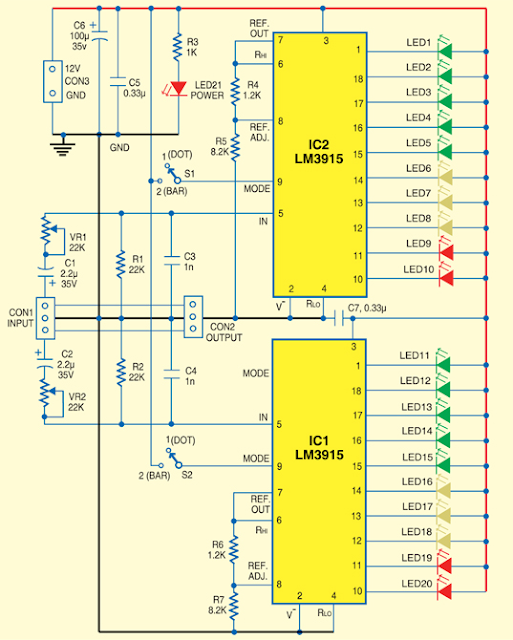
Automatic Low Power Emergancy Light Circuit diagram

Image
Here is a white-LED-based emergency light that offers the following advantages. 1-It is highly bright due to the use of white LEDs. 2-The light turns on automatically when mains supply fails, and turns off when mains power resumes. 3-It has its own battery charger. When the battery is fully charged, charging stops automatically. The charger power supply section is built around 3-terminal adjustable regulator IC LM317 (IC1), while the LED driver section is built around transistor BD140 (Q2). In the charger power supply section, an input AC main is stepped down by T1 to deliver 9V, 500mA to the bridge rectifier, which comprises diodes D1 through D4. Filter capacitor C1 eliminates ripples. Unregulated DC voltage is fed to input pin 3 of IC1 and provides charging current through D5 and limiting resistor R15. By adjusting preset P1, the output voltage can be adjusted to deliver the required charging current. When the battery gets charged to 6.8V, D6 conducts and charging current from IC1 fi...

Stereo Low power audio amplifier

Image
Audio amplifier circuit has a power output of 2 x 2.3 Watt, which uses IC KA2206, KA22061, LA4180, LA4182, LA4183, LA4550, LA4555, LA4558. The required voltage for at least 6 volts to 13 volts DC maximum. Component takes is a ic that I mentioned above one of them, and several capacitors elco. This Schematics low power amplifier Component Description C1 = 1uF C2 = 100uF C3 = 100uF C4 = 100uF C5 = 0.1uF C6 = 470uF C7 = 1uF C8 = 100uF C9 = 100uF C10 = 100uF C11 = 0.1uF C12 = 470uF ICs can use the ic which I mention above for each ic datasheet can be seen itself.

Low Power Transceiver Using by ADF7242

Image
This low power transceiver circuit project is designed using the ADF7242 fully integrated low-cost, short-range, low power transceiver designed for operation in the global 2.4 GHz ISM band.The receive path of the ADF7242 low power transceiver circuit is based on a zero-IF architecture enabling high blocking and selectivity performance. The transmit path is based on a direct closed loop VCO modulation scheme. The ADF7242 has a low consumption power that make it suitable for battery powered systems. Low Power Transceiver Circuit diagram The ADF7242 supports IEEE 802.15.4 compliant DSSS-OQPSK modulation with a bitrate of 250 kbps and also supports FSK and GFSK modulation with bitrates from 62.5 kbps to 2 Mbps.ADF7242 fully supports arbitrary data rates only for FSK mode of operation. The ADF7242 also has a built in battery monitor features that has a very low power consumption and may be used in parallel with any mode of operation, except SLEEP state. The battery monitor generates a batte...

Low Cost Stereo Level Indicator Circuit Diagram

Image
Usually, Low-Cost Stereo Level Indicator home stereo power amplifiers don’t have output level indicators . An output power level indicator can be added to each channel of these stereo power amplifiers . As low levels of the output power are not disturbing and damaging to the people, there is no need to add a preamplifier and low-level detector before IC LM3915. But you should know when the output power becomes considerably high. Here we present a very simple, low-cost stereo-level indicator circuit for home power amplifiers with power rating of around 0.5W. The circuit is built around two LM3915 dot/bar display driver ICs (IC1 and IC2). LM3915 senses analogue voltage levels to drive ten LEDs, providing a logarithmic 3dB/step analogue display. Stereo Level Indicator Circuit Diagram The voltage levels below 1V are not important because these correspond to a low level of the audio signal. Similarly, input voltage levels above 30V correspond to too high levels of the output power, which ...

Simple Low Distortion Audio Amplifier Circuit Diagram

Image
This is the Simple Low Distortion Audio Amplifier Circuit Diagram. The circuit was designed and sold as a card by a purveyor of surplus components but, even using mostly manufacturer's rejected transistors, we managed to get about 0.02% total harmonic distortion at 30 watts with a ±25v power supply into 8 ohms.: no bad figure even in these days of MOSFET and ICs. In 1977 anything below 0.1% was considered excellent. And this figure was pretty repeatable without doing much selection.  The problem of course is that since I haven't touched this amplifier for many a year I have absolutely no idea what modern transistor types one should use for it but they are not critical: output transistors and drivers need to be the correct type but the other transistors can be small signal types - as long as they can handle the full voltage between + and - supplies.  Simple Low Distortion Audio Amplifier Circuit Diagram   Tr1 and Tr2 are a long-tailed pair (LTP to save typing). It is quite...

stream powers low cost Macro Lens

Image
For all photography and video enthusiasts, a macro lens is quite simply a basic necessity. A macro lens is incredibly helpful to produce detailed pictures of tiny objects or options. despite the fact that nearly each photographer or video recorder wants one among these, they're quite expensive and hence not everybody will afford it. Nevertheless, there's the simplest way to create yourself a macro lens. Everything may be achieved by using any lens, 2 plastic bottles, super glue, and duct tape. A photography or video device to that the lens has got to be connected is additionally needed. 1st of all, the neck of a bottle is cut employing a hot knife. Another piece of plastic that's the same as the form of the bottle’s neck is cut out from a special bottle. This plastic section is placed at the lowest. This forms the bottom on that the lens can ought to be placed. The lens are held near the bottle neck using super glue. once holes are created at applicable positions at each en...

Low voltage Power Supply Circuit Diagram

Image
If you want to check the behaviour of an electronic circuit at low voltages, an adjustable power supply as shown here may be helpful. Powered from a 3 to 16 volts source (DC for sure), it will provide a stable output voltage in the 0 to 1.5 V range. Adjustable Low-voltage Power Supply Circuit Diagram Multiturn trimpot P1 allows the output volt-age to be adjusted with good precision. The BC337-400 output transistor raises the out-put current to about 200 mA bearing in mind that the minimum supply voltage is 3.5 V. The transistor’s dissipation should be taken into account, and a more power ful t ype used if necessary. T1 may be omitted and R2 replaced with a wire link if you are happy with 3 mA at 3 volts out, 10 mA at 6 V or 20-30 mA at 10-16 V. These values represent the maximum output current of the TLC271 op amp. Without T1, the minimum supply voltage is 3.0 V. Author:Vladimir Mitrovic - Copyright: Elektor

4A High Speed Low Side Gate Driver

Image
The UCC27518 and UCC27519 single-channel, high-speed, low-side gate driver device is capable of effectively driving MOSFET and IGBT power switches. Using a design that inherently minimizes shoot-through current, UCC27518 and UCC27519 are capable of sourcing and sinking high, peak-current pulses into capacitive loads offering rail-to-rail drive capability and extremely small propagation delay typically 17 ns. The UCC27518 and UCC27519 provide 4-A source, 4-A sink (symmetrical drive) peak-drive current capability at VDD = 12 V. The UCC27518 and UCC27519 are designed to operate over a wide VDD range of 4.5 V to 18 V and wide temperature range of -40°C to 140°C. Internal Under Voltage Lockout (UVLO) circuitry on VDD pin holds output low outside VDD operating range. Features Low-Cost, Gate-Driver Device Offering Superior Replacement of NPN and PNP Discrete Solutions Pin-to-Pin Compatible With TI’s TPS2828 and the TPS2829 4-A Peak Source and 4-A Peak Sink Symmetrical Drive Fast Propagati...

500W low cost 12V to 220V inverter

Image
Using this circuit you can convert the 12V dc in to the 220V Ac. In this circuit 4047 is use to generate the square wave of 50hz and amplify the current and then amplify the voltage by using the step transformer.   Circuit diagram   How to calculate transformer rating The basic formula is P=VI and between input output of the transformer we have Power input = Power output For example if we want a 220W output at 220V then we need 1A at the output. Then at the input we must have at least 18.3V at 12V because: 12V*18.3 = 220v*1 So you have to wind the step up transformer 12v to 220v but input winding must be capable to bear 20A. author: Ashad Mustufa e-mail: mustufa66@hotmail.com Source : http://www.electronics-lab.com

Low Cost Step Down Converter

Image
The circuit described here is mostly aimed at development engineers who are looking for an economical step-down converter which offers a wide input volt-age range. As a rule this type of circuit employs a step-down converter with integrated switching element. However, by using a more discrete solution it is possible to reduce the total cost of the step-down converter, especially when manufacturing in quantity. The TL5001A is a low-cost PWM controller which is ideal for this project. Low Cost Step Down Converter with Wide Input Voltage Range The input voltage range for the step-down converter described here is from 8 V to 30 V, with an output voltage of 5 V and a maximum output current of 1.5 A. When the input voltage is applied the PWM output of IC1 is enabled, taking one end of the voltage divider formed by R1 and R2 to ground potential. The cur-rent through the voltage divider will then be at most 25 mA: this value is obtained by dividing the maximum input voltage (30 V) minus t...

3khz Low Pass Filter and Audio Amplifier Circuit Diagram

Image
This circuit uses a switched capacitor filter IC from National Semiconductor to filter signals with frequencies higher than the 3KHz needed for voice audio. The schematic includes an audio amplifier that is designed to drive a standard audio head phone.  The circuit is described in more detail in the receiver section of Dave Johnson's Handbook of Optical Through the Air Communications.(this link is off-site)  3khz Low Pass Filter and Audio Amplifier Circuit Diagram  

Low Noise Microphone preamplifier

Image
This circuit use to raise the gain to reduce noise or amplify the signal. And this circuit use IC OP27 / OP37 , this is precision opertional amplifier ,lower noise , and higher speed with the  same input ofset with drift specifications as the OP07 . Both parts have a 10 uV offset , 0.2 uV drift , and 1.8 million gain. Coupled with low voltage noise of 3.5 nV  at 10 Hz and a low 1 /f noise corner frequency of 2.7 Hz, the  OP27 / OP37 are optimized for accurate amplification of low - level signal.  See schematic and pin configuration below : Click to view Larger Output swing about 10 V into 600 Ohm. Input voltage maximum 25 V. This circuit also can use to , Low noise DC amplifiers , Microphone Amplifiers , Precision Amplifier , Tape - Head  Preamplifiers , Termocouple Amplfiers , Low - level Signal Processing , Medical instrumentation m Strain - gauge Amplifiers , High accuracy Data Acquistion.

2 3 Watt Low audio power amplifier

Image
These amplifiers using IC KA2202 and KA2207, which has a power output of 2.3 Watt berimpedansi 4 ohms. Minimum supply voltage and maximum 5Volt 20Volt. See schematics and component list below. Part List  R1 = 100K R2 = 56R R3 = 56R R4 = 1R Use 1/4 Watt resistor C1 = 100uF C2 = 100uF C4 = 100uF C5 = 470uF C6 = 100nF C7 = 470pF C8 = 2,2nF C9 = 100uF U1 = KA2202 , KA2207

Step Down Converter With Wide Input Voltage Range

Image
The circuit described here is mostly aimed at development engineers who are looking for an economical step-down converter which offers a wide input voltage range. As a rule this type of circuit employs a step-down converter with integrated switching element. However, by using a more discrete solution it is possible to reduce the total cost of the step-down converter, especially when manufacturing in quantity. The TL5001A is a low-cost PWM controller which is ideal for this project. The input voltage range for the step-down converter described here is from 8 V to 30 V, with an output voltage of 5 V and a maximum output current of 1.5 A. When the input voltage is applied the PWM output of IC1 is enabled, taking one end of the voltage divider formed by R1 and R2 to ground potential. The current through the voltage divider will then be at most 25 mA: this value is obtained by dividing the maximum input voltage (30 V) minus the saturation voltage of the output driver (2 V) by the total resi...

Battery Switch With Low Dropout Regulator Project

Image
In the form of the LT1579 Linear Technology (www.linear-tech.com) has produced a practical battery switch with an integrated low-dropout regulator. In contrast to previous devices no diodes are required. The circuit is available in a 3.3 V version (LT1579CS8-3.3) and in a 5 V version (LT1579CS8-5), both in SO8 SMD packages. There is also an adjustable version and versions in an SO16 package which offer a greater range of control and drive signals. The main battery, whose terminal voltage must be at least 0.4 V higher than the desired output voltage, is connected to pin IN1. The backup battery is connected to pin IN2. The regulated output OUT can deliver a current of up to 300 mA. The LDO regulator part of the IC includes a pass transistor for the main input voltage IN1 and another for the backup battery on IN2.  Battery Switch With Low-Dropout Regulator circuit Diagram The IC will switch over to the backup battery when it detects that the pass transistor for the main voltage input ...

Low Power Wireless Audio Power Amplifier

Image
Using this low-cost project one can reproduce audio from TV without disturbing others. It does not use any wire connection between TV and Loud Speaker. In place of a pair of wires, it uses invisible infra-red light to transmit audio signals from TV to Loud speakers, Without using any lens a range of up to 6 meters is possible. Range can be extended by using lenses and reflectors with IR sensors comprising transmitters and receivers. Transmitter's operation: IR transmitter uses two-stage transistor amplifier to drive two series-connected IR LEDs. An audio output transformer (T1) is used (in reverse) to couple audio output from TV to the IR transmitter. Transistors Q1 and Q2 amplify the audio signals received from TV through the audio transformer. Low impedance output windings (lower gauge or thicker wires) are used for connection to TV side while high-impedance windings are connected to IR transmitter. This IR transmitter can be powered from a 9V mains adapter or a 9V battery. Red L...