Electronic Digital Combination lock Circuit Diagram

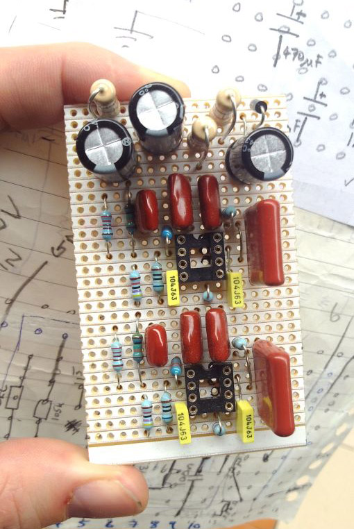
The circuit above above makes use of the CMOS 4017 decade counter IC. Each depression of a switch steps the output through 0– 9. By coupling the output via an AND gate to the next IC, a predefined code has to be input to create the output. Each PBS switch is de bounced by tw1o gates of a CMOS4001 quad 2-input NOR gate. This ensures a clean pulse to the input of each CMOS4017 counter. Only when the correct number of presses at PBS Awill allow PBS B to become active. This is similar for PBS C and PBS D. At IC4, PBS D must be pressed 7 times. Then PBS C is again pressed 7 times, stepping from output 1 to output 8. The AND gate formed around CMOS4081 then goes high, lighting the LED. The Reset switch can be pressed at any time. Power on resetis provided by the 100n capacitor near the reset switch. Below is a picture of one that I made about 15 years ago:

Unfortunately, this board was part of a much larger project containing multiple power supplies. One day whilst working on another circuit , I slipped with a wire and splashed 24volts DConto this board. There was a small spark, and puff of smoke before all this chips were cooked! If anyone does consider building such a circuit, then my advice would be to stop and lookin your local electronic parts catalogue. There are now dedicated combination lock IC`s with combinations many time sgreater than this circuit. Incidentally the number of combinations offered here is 10 x 10 x 10 x 10 x 9 = 90,000.Check out Dean White`s Electronic Gadgets, on the Electronic Sites Alliance web ring, he also has a combination lock circuit.


Comments
Post a Comment